강달영 연구실
연세대학교 신소재공학과
강달영 교수
강달영 교수 연구실
홈
강달영 연구실
연세대학교 신소재공학과 강달영 교수
강달영 연구실은 신소재공학과 재료공정공학을 기반으로 신축성·폴더블 전자소자, 실리콘 미세구조 가공, 전사 프린팅, 하이브리드 태양전지 및 광전자 소재를 연구하며, 특히 저온·대면적 공정과 계면·표면 공학을 통해 차세대 전자소자와 에너지 소자의 성능 및 제조 가능성을 동시에 높이는 융합형 재료 연구를 수행하고 있다.
대표 연구 분야
연구 영역 전체보기
신축성·폴더블 전자소자 및 전사 프린팅
신축성·폴더블 전자소자 및 전사 프린팅
실리콘 미세·거대 구조화와 금속보조 화학식각
하이브리드 태양전지와 저온 공정 기반 에너지 소재
주요 논문
5
논문 전체보기
1
review
|
인용수 80
·
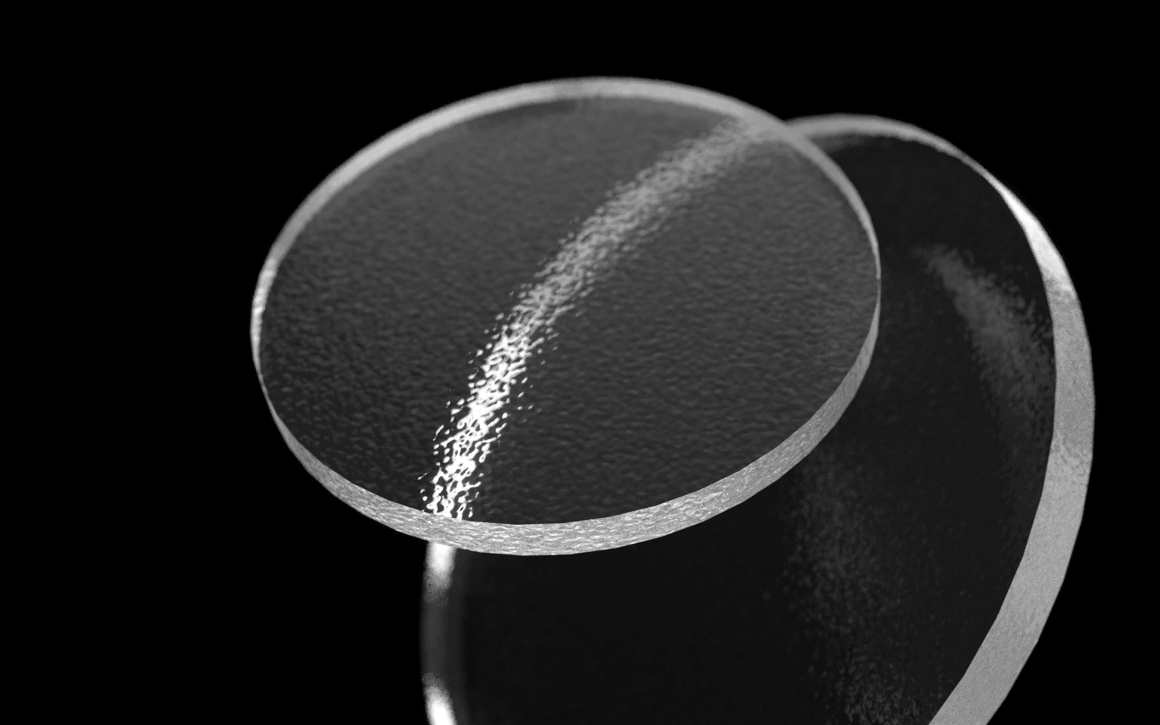
2021Structuring of Si into Multiple Scales by Metal‐Assisted Chemical Etching
R. P. Srivastava, Dahl‐Young Khang
IF 26.8
Advanced Materials
Structuring Si, ranging from nanoscale to macroscale feature dimensions, is essential for many applications. Metal-assisted chemical etching (MaCE) has been developed as a simple, low-cost, and scalable method to produce structures across widely different dimensions. The process involves various parameters, such as catalyst, substrate doping type and level, crystallography, etchant formulation, and etch additives. Careful optimization of these parameters is the key to the successful fabrication of Si structures. In this review, recent additions to the MaCE process are presented after a brief introduction to the fundamental principles involved in MaCE. In particular, the bulk-scale structuring of Si by MaCE is summarized and critically discussed with application examples. Various approaches for effective mass transport schemes are introduced and discussed. Further, the fine control of etch directionality and uniformity, and the suppression of unwanted side etching are also discussed. Known application examples of Si macrostructures fabricated by MaCE, though limited thus far, are presented. There are significant opportunities for the application of macroscale Si structures in different fields, such as microfluidics, micro-total analysis systems, and microelectromechanical systems, etc. Thus more research is necessary on macroscale MaCE of Si and their applications.
https://doi.org/10.1002/adma.202005932
Materials science
Structuring
Nanotechnology
Mace
Fabrication
Microelectromechanical systems
Etching (microfabrication)
Nanoscopic scale
Nanomaterials
Scalability
2
article
|
인용수 73
·
2017High Efficiency (>17%) Si‐Organic Hybrid Solar Cells by Simultaneous Structural, Electrical, and Interfacial Engineering via Low‐Temperature Processes
Sungsoo Yoon, Dahl‐Young Khang
IF 26
Advanced Energy Materials
Abstract Highly efficient organic–inorganic hybrid solar cells of Si‐poly(3,4‐ethylenedioxythiophene):polystyrene sulfonate (PEDOT:PSS) have been demonstrated by simultaneous structural, electrical, and interfacial engineering with low processing temperature. Si substrate has been sculpted into hierarchical structure to reduce light reflection loss and increase interfacial junction area at the same time. Regarding the electrical optimization, highly conductive organic PEDOT:PSS layer has been formulated with low sheet resistance. It is argued that the sheet resistance, rather than conductivity, is the primary parameter for the high efficiency hybrid cells, which leads to the optimization of thickness, i.e., thick enough to have low sheet resistance but transparent enough to pass the incident sunlight. Finally, siloxane oligomers have been inserted into top/bottom interfaces by contact‐printing at room ambient, which suppresses carrier recombination at interfaces and reduces contact resistance at bottom electrode. Contrary to high‐temperature doping (for the formation of front surface or back surface fields), wet solution processes or vacuum‐based deposition, the contact‐printing can be done at room ambient to reduce carrier recombination at the interfaces. The high efficiency obtained with low processing temperature can make this type of cells be a possible candidate for post‐Si photovoltaics.
https://doi.org/10.1002/aenm.201702655
Materials science
PEDOT:PSS
Sheet resistance
Contact resistance
Organic solar cell
Optoelectronics
Polystyrene sulfonate
Substrate (aquarium)
Electrical conductor
Polystyrene
3
article
|
인용수 50
·
2015Glass and Plastics Platforms for Foldable Electronics and Displays
Moon Jong Han, Dahl‐Young Khang
IF 26.8
Advanced Materials
Reversibly, repeatedly foldable electronics and displays are enabled by employing engineered glass or plastics substrates, where folding deformation is localized in thinned parts only. This design concept can further be extended to dual folding, leading to size reduction down to 1/4. Notably, the foldable electronics and displays can be implemented with no need to introduce any novel materials.
https://doi.org/10.1002/adma.201501060
Materials science
Electronics
Folding (DSP implementation)
Nanotechnology
Flexible electronics
Flexible display
Dual (grammatical number)
Optoelectronics
Mechanical engineering
Thin-film transistor
정부 과제
7
과제 전체보기
1
주관|
2017년 5월-2019년 5월
|12,500,000원유연 양면형 실리콘-유기물 하이브리드 태양전지
본 과제는 구부리거나 접을 수 있는 양면형 Si-유기물 하이브리드 태양전지를 개발하는 연구임.
연구목표는 Si의 미세 구조화로 수직적 구조 하이브리드 태양전지를 제조하고, 유연고분자 복합체로 folding/bending 같은 외력에도 성능을 유지하는 태양전지 개발이며, 상/하부 투명전극으로 양쪽에서 태양광 입사 가능한 양면형 유연 구조 구현임. 핵심연구내용은 습식식각 Si pillar 및 투명고분자 복합체 공정, 유기물 박막·상/하부 투명전극 형성, 입사 방향 및 약한 입사광 성능 분석, 곡률반경·folding radius에 따른 내구성 및 변환효율 10% 이상 최적화임. 기대효과는 고효율 태양전지의 저비용 제조 및 휴대용 보조전원 상용화 가능성 향상, orthogonalized 구조 기반의 원천기술·원천특허 확보 및 다양한 유연 전자소자 적용임.
실리콘-유기물 하이브리드 태양전지
유연 태양전지
양면형 태양전지
2
주관|
2010년 9월-2016년 9월
|90,000,000원수처리용 혁신 분리막 패터닝용 마스터 몰드 개발
본 과제는 분리막 표면에 매우 작은 패턴을 새겨 물이 더 잘 통과하고 오염이 덜 붙는 차세대 혁신 분리막을 만들기 위해 필요한 마스터 몰드 제작 기술을 개발하는 연구임.
연구 목표는 미세패턴 형성을 위한 마스터 몰드 제조공정 확립에 있음. 핵심 내용은 나노패턴 마스터 몰드의 저가·대면적 제조공정 탐색, 전기화학적 식각을 통한 형상 제어, 규칙적·무질서 나노와이어 성장 제어, CFD 기반 패턴 최적화, 대면적 나노패턴 균일도 향상 및 롤 프린팅 기반 대형화 시도임. 기대 효과는 세계 최초 수준의 나노패턴 분리막 원천기술 확보와 고성능 분리막 국산화, 다양한 수처리 및 오염저감 분야로의 응용 확대, 해외시장 개척을 통한 경제적 가치 창출임.
나노패턴 분리막
마스터 몰드
나노와이어
전기화학적 식각
무인쇄 접촉 프린팅
롤 프린팅
3
주관|
2010년 9월-2016년 9월
|105,000,000원수처리용 혁신 분리막 패터닝용 마스터 몰드 개발
표면에 미세패턴을 갖는 차세대 혁신 분리막의 제조에 있어 미세패턴 복제용 마스터 몰드의 개발을 본 연구의 주 내용으로 하며, 연구의 구제적인 내용은 다음과 같다.
(가) 나노패턴 마스터 몰드 제조 공정
- 문헌조사를 통한 나노패턴 몰드의 저가, 대면적 제조공정 스크리닝
- 전기화학적 식각공정 장치 set-up 구체화
(나) 전기 화학적 식각 공정 개발
- 금속 촉매의 종류, 형상 등에 따른 마스터 몰드 형상 제어
- 전기화학적 식각 공정 변수에 따른 마스터 몰드 형상 제어
(다) 규칙적 나노와이어 몰드 제조 공정
- 콜로이드 입자를 이용한 규칙적 나노와이어 성장 제어
(라) 나노패턴 몰드 형상 최적화
- 분리막 실험 및 CFD 결과의 feedback을 통한 나노패턴 몰드 형상 최적화
- 이형문제 및 미세패턴의 기계적 안정성 평가를 통한 나노패턴 몰드 형상 최적화
(마) 나노패턴 마스터 몰드의 대면적화
- 대면적(>10cm*10cm) 나노패턴 마스터 몰드 제조 공정 개발
- 나노패턴 균일도 향상 연구
- 롤 프린팅 기법을 적용한 마스터 몰드의 대형화 시도
나노패턴 분리막
마스터 몰드
나노와이어
전기화학적 식각
무인쇄 접촉 프린팅
롤 프린팅
최신 특허
특허 전체보기
전체 특허
사용후 복합 기능성 세라믹볼 혹은 구조체 세척방법
상태
등록출원연도
2024출원번호
1020240022529우조 에멀션을 이용한 고분자 나노 구조체 제조방법
상태
공개출원연도
2024출원번호
1020240021611청색광 페로브스카이트 나노입자 및 그의 제조 방법
상태
등록출원연도
2021출원번호
1020210179937